The active detection elements of the UT consist of almost 1000 silicon microstrip sensors.

The sensors were manufactured by Hamamatsu Photonics following designs produced by Syracuse. All sensors were tested and used to construct the detector at Syracuse. There are four designs, with increasing segmentation towards the beam where more particles pass through.
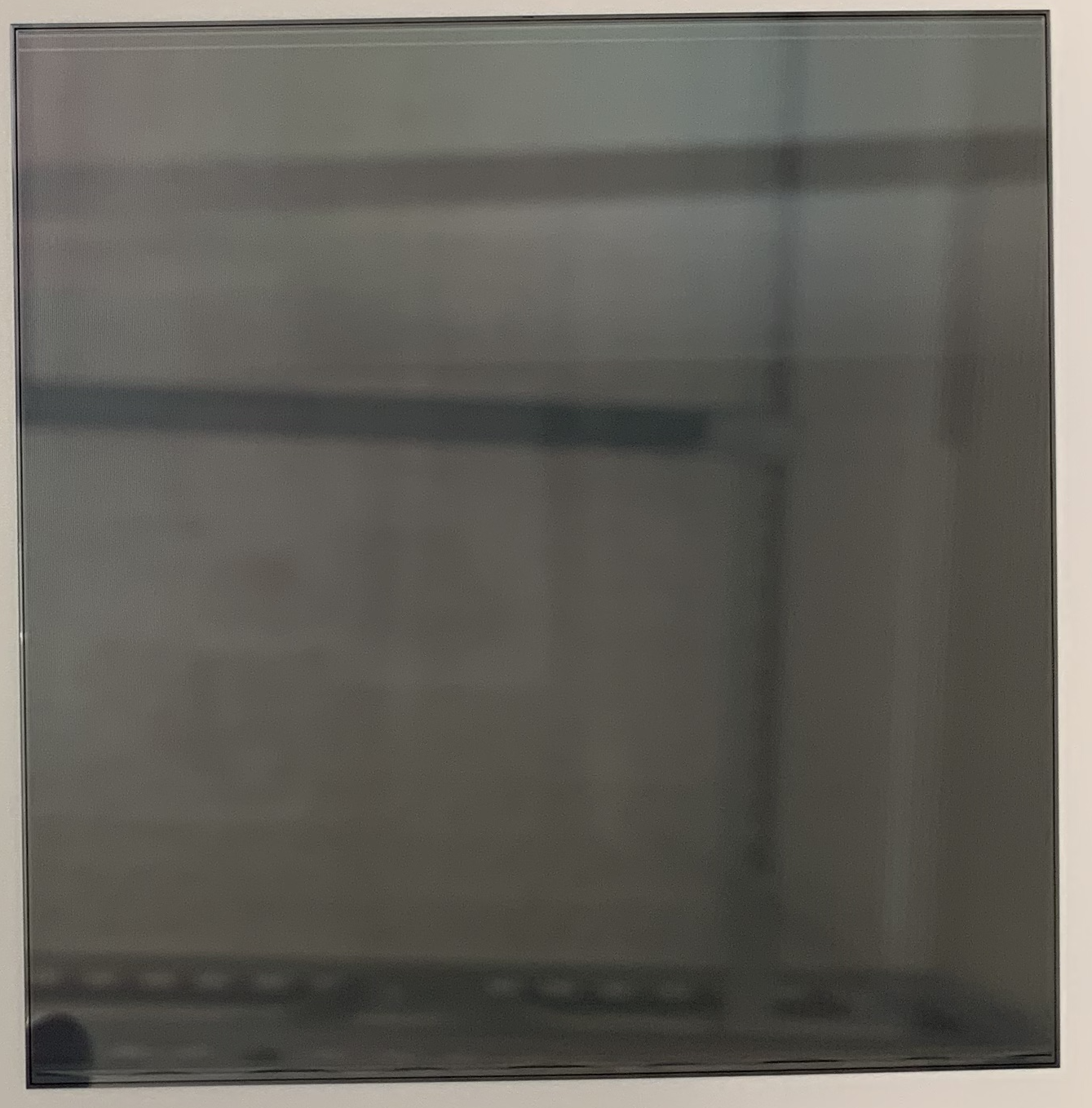
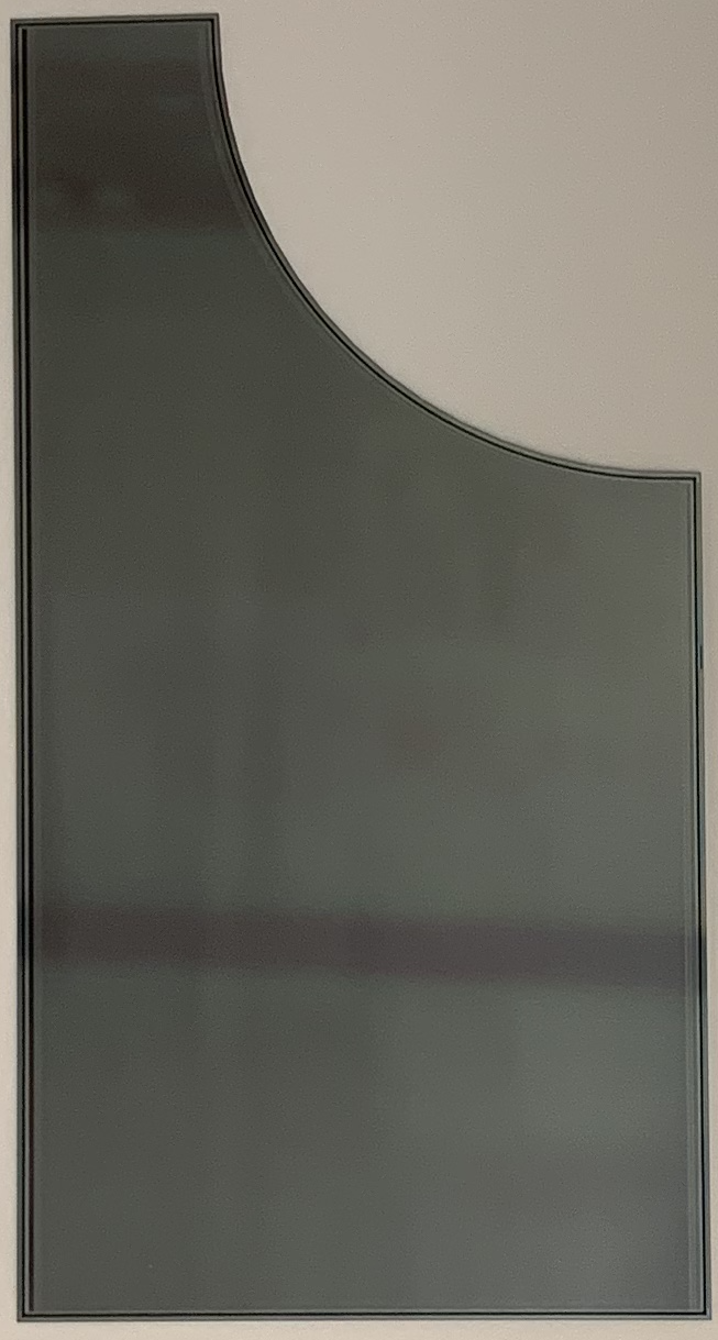
Most of the detector uses 320 μm thick Type A sensors, each with an area of approximately 10 cm x 10 cm. The active area is segmented into independent detection elements (or strips), each with a width of less than 200 μm.

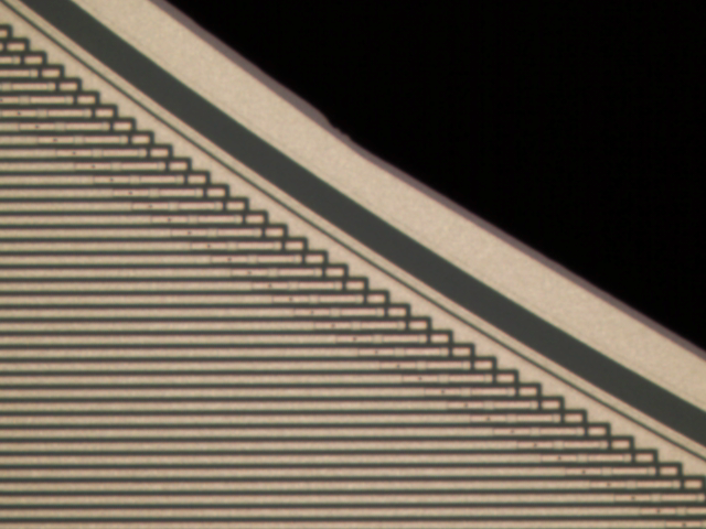
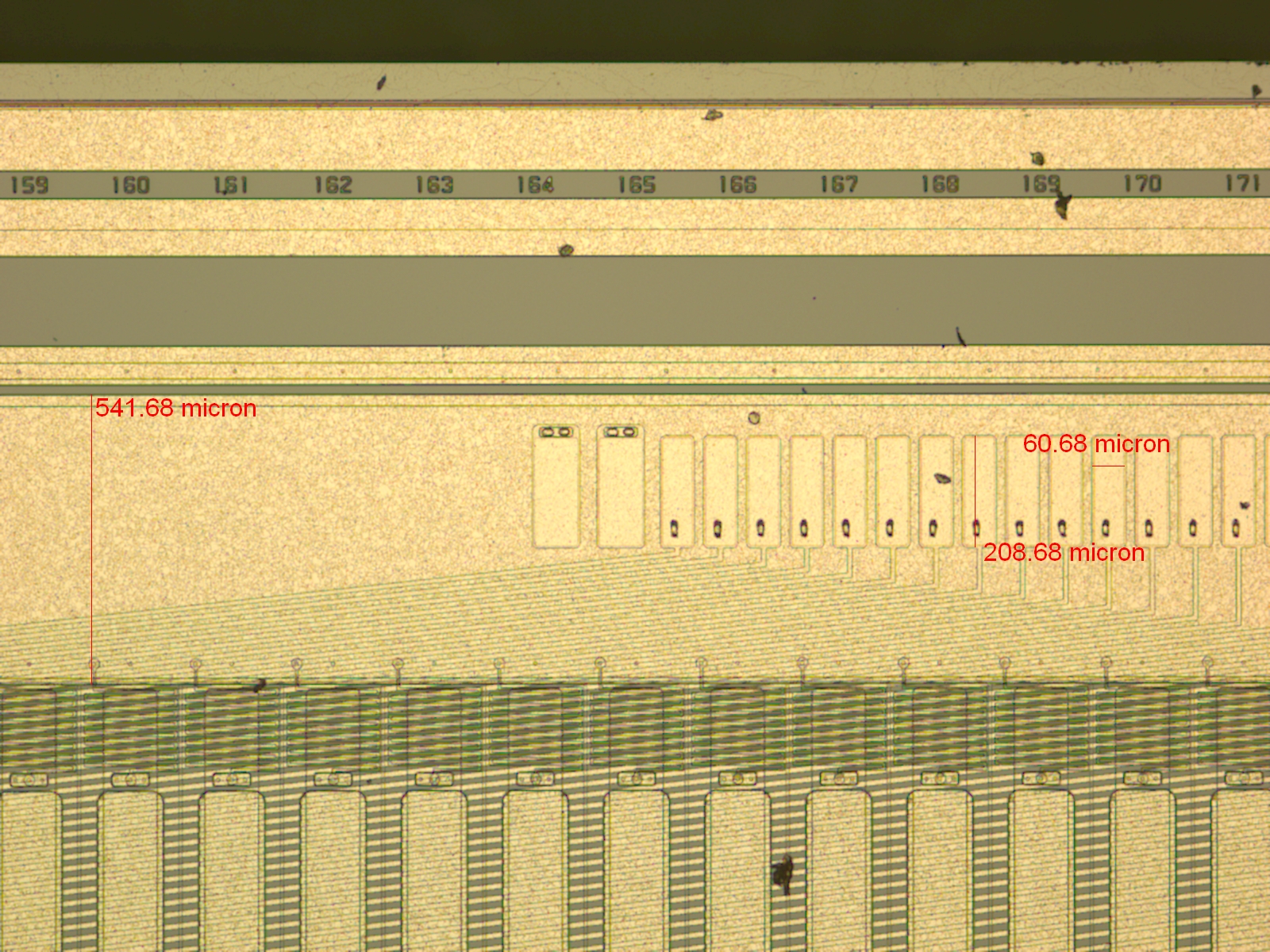
When charged particles pass through the sensor, currents are detected on the nearest strip(s). To facilitate the connection of the 200 μm-spaced strips to the
80 μm pad spacing on the readout electronics, an embedded pitch adapter is formed using a second metal layer on top of the strips. With matched spacing between the silicon pads and the readout electronics pads, the wirebonding is simpler and more robust.
The innermost part of the UT detector (closest to the beam pipe) uses sensors with strips about 100 μm apart. Type B sensors are still 10 cm x 10 cm in size, but Type C and D sensors use shorter strips — about 5 cm long — to reduce the hit occupancy close to the beam pipe.