

The UT silicon-strip sensors include several novel features:
- A double-metal layer for pitch adapting: A double-metal layer where the sensor pitch is fanned in from the 190 um sensor strip pitch to 80 um to match the SALT front end pad spacing.
- Topside biasing: The sensor has a bias pad on the top of the sensor, and the bias voltage is brought to the backside of the sensor through an active edge.
- Circular cutout in Type D sensors: To maximize the acceptance, the innermost (Type D) sensors have a circular cutout to match the contour of the beam pipe.
More information about the UT sensors and these novel features can be found here.
A multi-year testbeam effort was carried out to test specific features of the UT sensors, as well as baseline properties such as the signal-to-noise ratio (S/N), efficiency (both integrated and versus position in sensor), cluster sizes, and resolution, for both unirradiated and heavily irradiated sensors. Below, we discuss a few of the results. More details can be found in the embedded links and the references at the end.
In total, nine separate testbeam campaigns were carried out over a 6-year period. The first such test was conducted at the proton synchrotron at CERN. The next 7 beam tests were carried out at the SPS at CERN, and the last one at the Fermilab Test Beam Facility (FTBF). The first 8 testbeams used the Beetle readout chip, the chip used for the LHCb Run 1 & Run 2 silicon detectors, since the SALT chip was not available at that time.The last beam test at FTBF used the 128-channel SALT v3.0 chip.
The left figure below shows the setup at the first SPS test beam at CERN. The box in the middle houses the detectors under test (DUT), a pair of mini-sensors (about 1.4 cm x 1.4 cm each). The box is on a stage that allows for translations and rotation for alignment and to study charge sharing versus angle. To the left and right of the DUT is the TimePix3 telescope , which provides a precise measurement of the beam tracks passing through the DUT. Numerous studies were performed, and the results are published in Nucl. Instrum and Methods 806, 244-257 (2016) (also available as an LHCb Public Note). The figure to the right shows the mini-sensors tested. Two of the sensors have a scaled version of the 1/4-circle cutout that will be on the final 10 cm x 10 cm full-size sensors. (Click on images for enlarged versions)
The figure below shows the distribution of collected charge on an n-in-p type mini-sensor that has been irradiated to a fluence of 4.0 x 10¹⁴ neq/cm2 (23.3 MRad), for increasing bias voltage on the sensor. The distributions are fit to a Landau distribution convolved with a Gaussian function. The most probable value (MPV), Landau width and Gaussian noise parameters are indicated.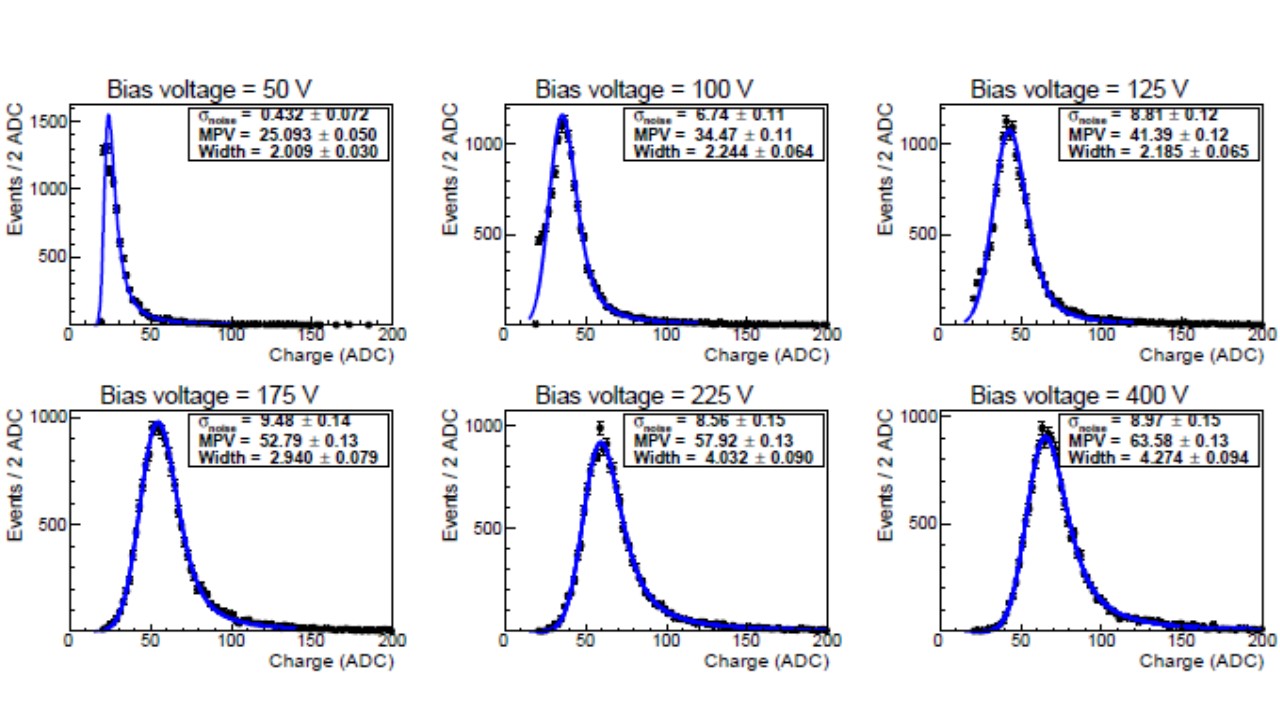
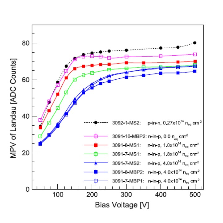
This figure summarizes the MPV of collected charge as a function of the bias voltage for several of the mini-sensors tested, from unirradiated up to 4.0 x 10¹⁴ neq/cm2 (23.3 MRad). The trend is clear that as the level of irradiation increases, less charge is collected. This is likely due to point defects in the silicon lattice that leads to charge being trapped.
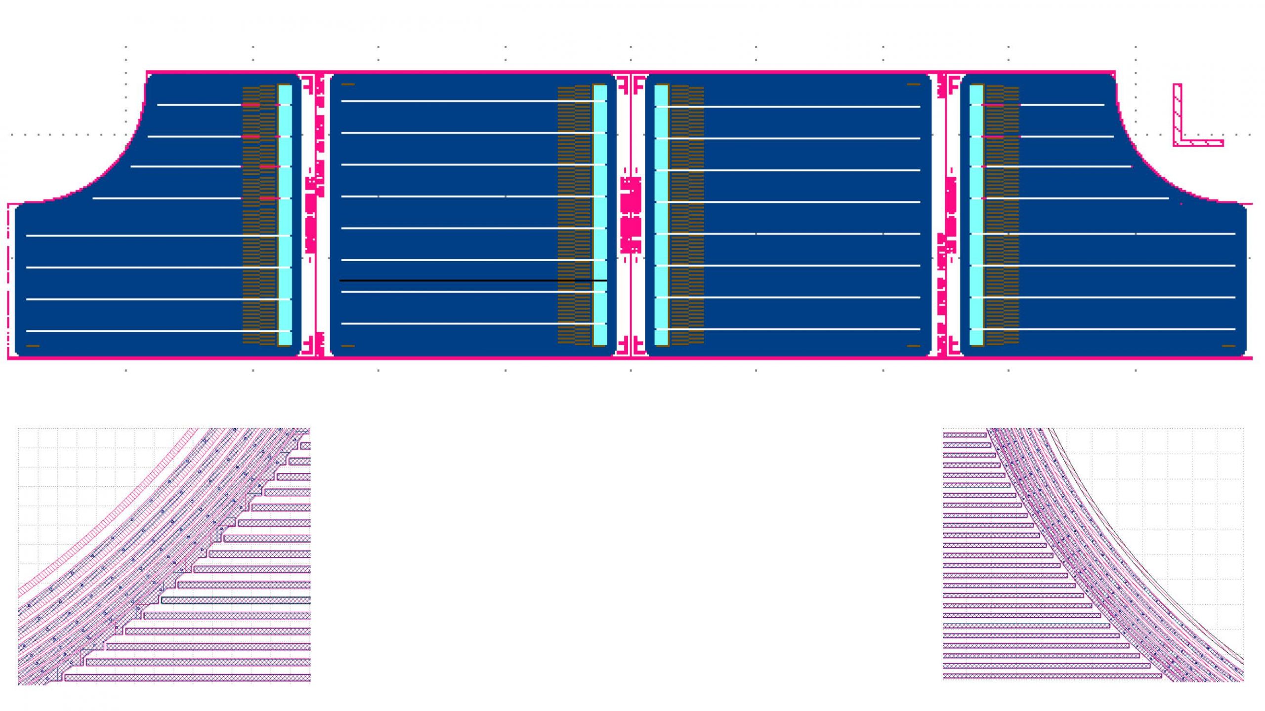
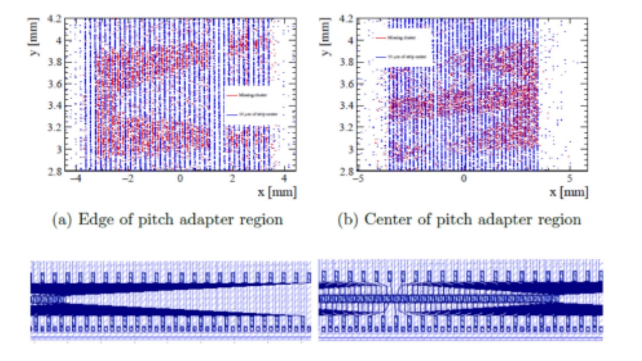
In 2015, an extensive beam test was carried out on several full size sensor sensor prototypes. The studies are documented in an LHCb Public Note. One of the key R&D questions was whether there was any loss of signal efficiency in the double-metal region of the sensor. Using well defined tracks from the TimePix3 telescope, we investigated how often a hit was found or not found in the DUT as a function of the (X,Y) coordinate, in the vicinity of the double-metal layer. The results are shown below. The top row show the positions of tracks when there is no hit found in the DUT (red points). The blue vertical bands show the positions of tracks when there is a hit found within 10 um of the center of the silicon strip. The bottom row shows the layout of the pitch adaptor region. A significant inefficiency is observed when a charged particle passes near to the middle between two strips in the double-metal region of this prototype sensor. Although this pitch adapting region is only a few percent of the active area of the sensor, this loss in efficiency (up to 90% loss) was deemed unacceptable. Other studies on topside versus backside biasing, S/N, efficiency of the circular cutout region, along with additional information can be found in the LHCb Public Note.
A deeper understanding of the charge loss was gleaned through additional analysis and detailed simulations. It was shown that the deposited charge was not being fully collected on the nearest 1-2 strips, but was capacitatively coupling to other strips, and being shared among many strips. Thus too little charge was detected on the expected strip to declare it as a valid hit. Those studies were published in Nucl. Instrum. Meth A877 , 252-258 (2018) [arXiv:1708.03371].
Changes to the sensor design were made to ameliorate these efficiency losses, and subsequent tests showed that there was no significant loss of efficiency in the region of the pitch adaptor. Details of these modifications are discussed on this page.
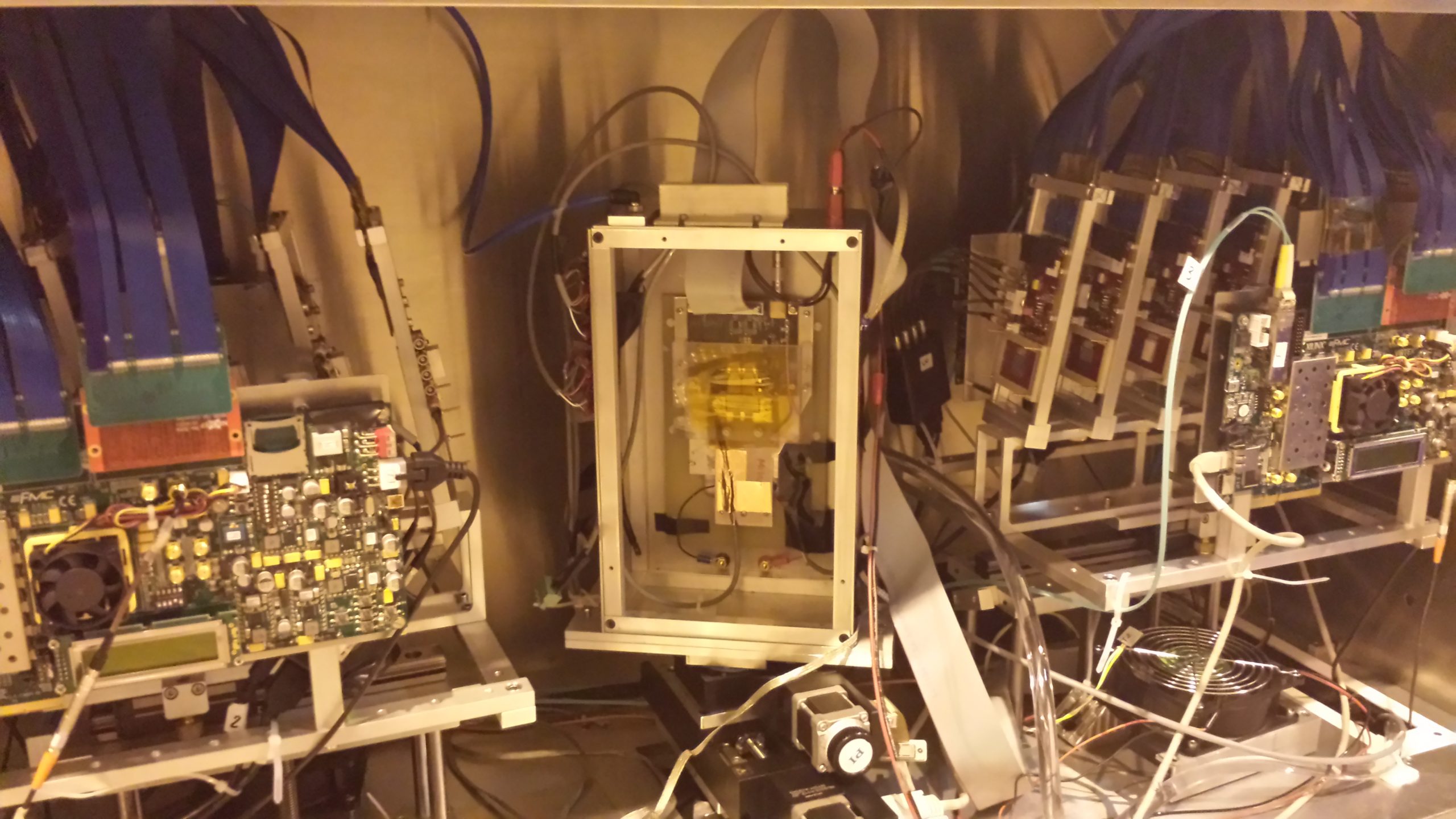
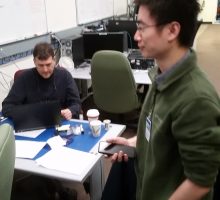
The last beam test was conducted at the Fermilab Test Beam Facility at Fermilab using a production-grade Type A sensor and an early version of the SALT 128-channel chip (SALT v3.0). The setup in the beam is shown at the top of this page. The FTBF telescope was used to provide the trajectories of the beam particles incident on the DUT. Due to large noise pickup in the region of the FTBF telescope, the hit thresholds in the DUT were set at 6 ADC counts, which is larger than the value of 3-4 ADC threshold we expect to use in LHCb. (Note: the #e-/ADC is not the same between the Beetle chip and the SALT chip)
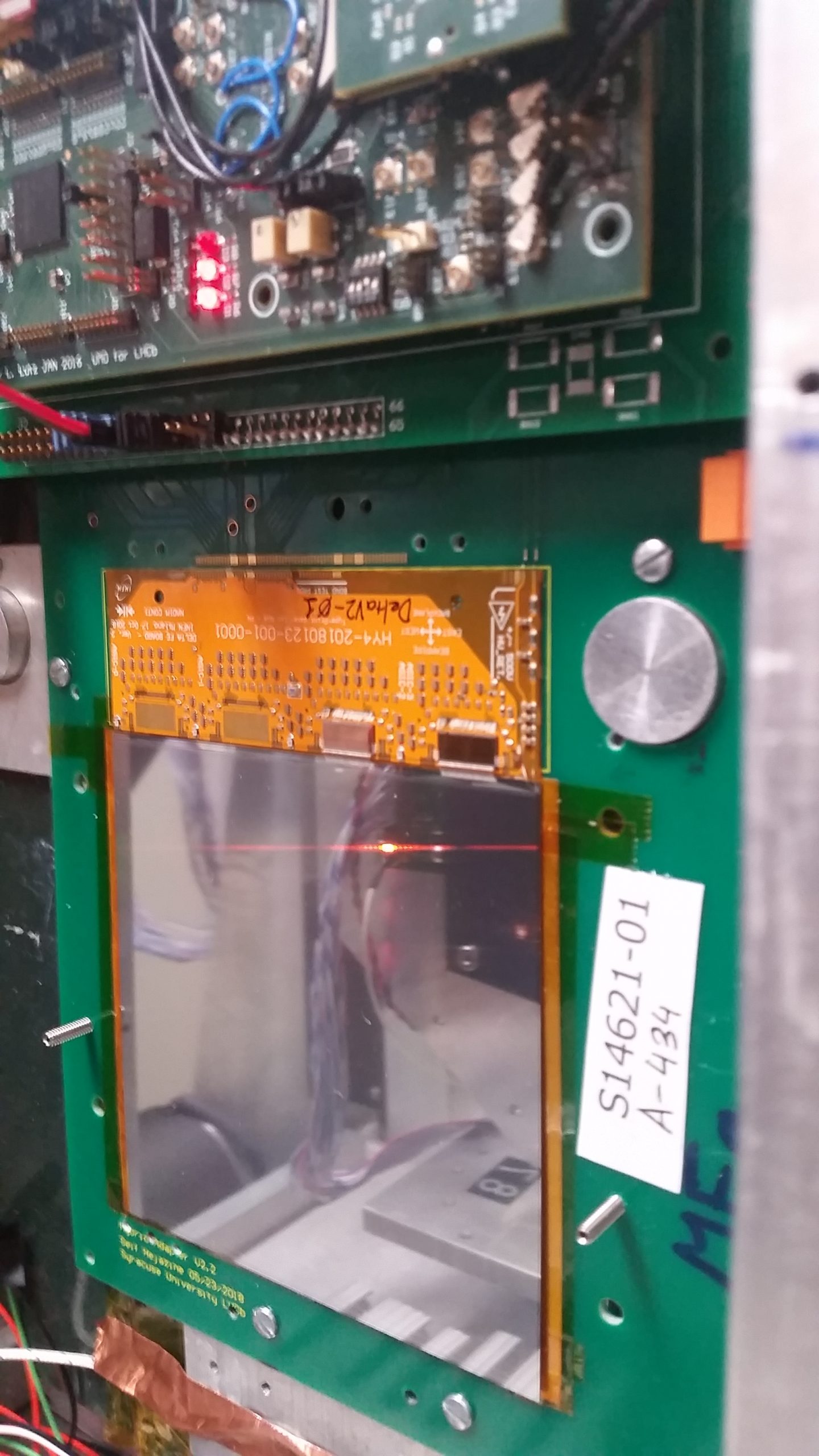
The photo shows a Type A sensor being tested at the FTBF. The sensor is clearly visible, and just above it is the hybrid. The sensor & hybrid are mounted on a carrier board, which is in turn connected to additional boards for reading out the detector.
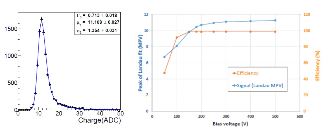
Below, we show (left) the distribution of collected charge on a Type A sensor at 300 V, where a mean of about 11.1 ADC counts is obtained. The graph to the right shows the MPV vs bias voltage and the hit efficiency versus bias voltage. We see that in the plateau region (above about 250 V), the hit efficiency is about 100%, and the signal approaches about 11.5 ADC counts. From an independent measurement, the common-mode subtracted noise is about 0.85 – 0.90 ADC counts. Thus, we expect a S/N of close to 13 for Type A sensors. At the maximum expected fluence, it is expected that the signal will drop by about 10-15% with no change in the noise; thus a S/N closer to about 11 is expected as we approach the targeted integrated luminosity at LHCb of ~50 fb-1 by 2030.
 Measurements on Type D sensors (10 cm x 5 cm in size, with a 1/4-circle cutout) were also carried out and for these shorter strips, the S/N is about 18. The efficiency near the 1/4-circle cut in the sensor was also investigated, and there is no observable loss of hit efficiency as one approaches the boundary.
For the UT, hit resolution is not a critical issue. With the strip pitch being about 93.5 um or 187.5 um, most hits (~90%) leave charge only on a single strip. In this case, the resolution is simply the strip pitch divided by √12. The testbeam measurements are consistent with this expectation. For about 10% of hits, the charge is shared, and in this case, charge weighting can provide improved position resolution.
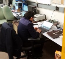
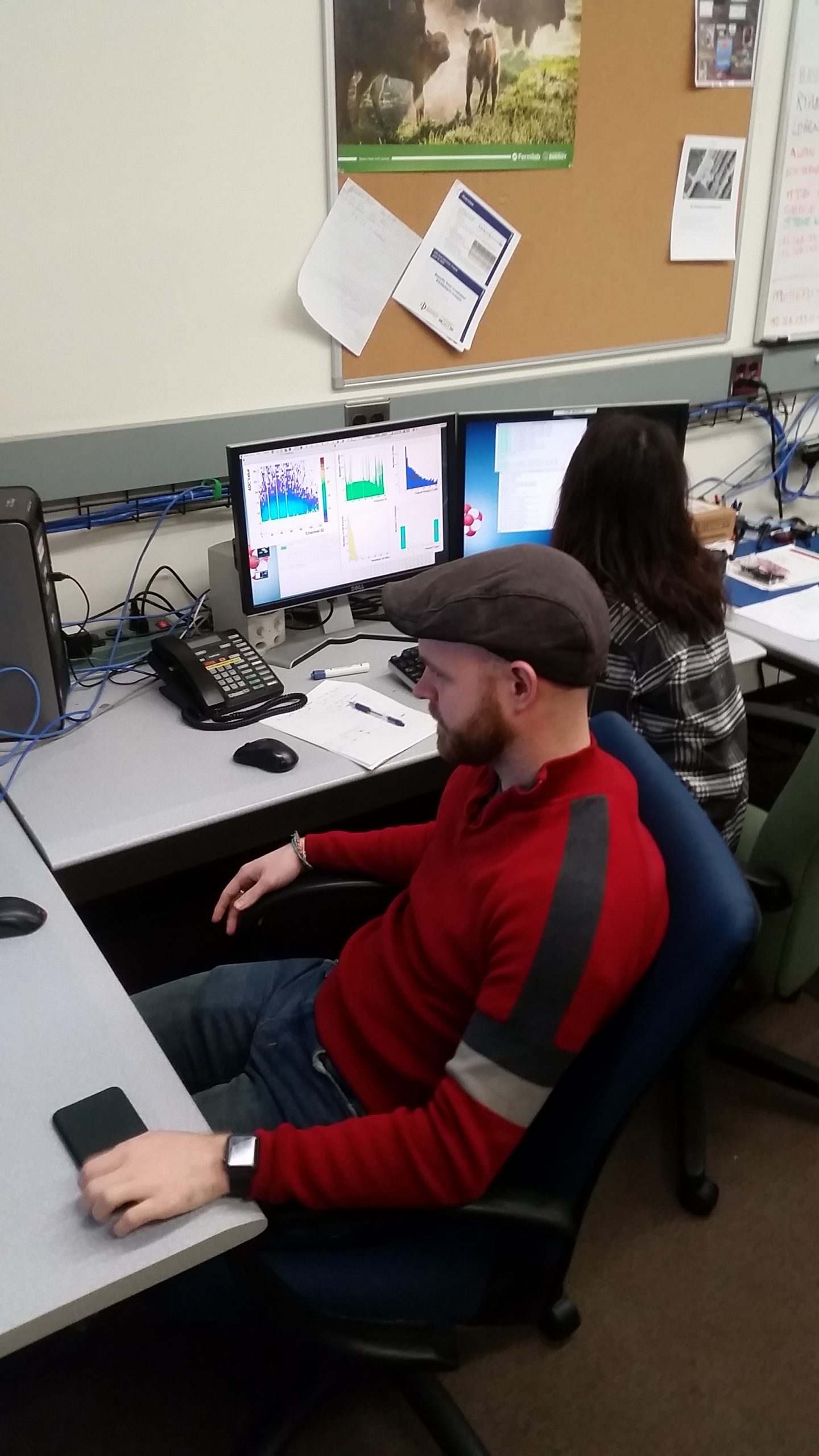
Below, we show some of the actors carrying out the measurements at Fermilab. From left to right is JC Wang, Steve Blusk, Zhuoming Li, Michael Wilkinson and KyungEun Kim.
References
-
A. Abba et. al., Testbeam studies of pre-prototype silicon strip sensors for the LHCb UT upgrade project, Nucl. Instrum. Meth A806, 244-257 (2016), arXiv:1506.00229, LHCb-PUB-2015-015.
-
A. Abba et. al., Study of prototype sensors for the Upstream Tracker Upgrade, LHCb-PUB-2016-007.
-
M. Artuso et. al., First beam test of UT sensors with the SALT 3.0 readout ASIC, LHCb-PUB-2019-009.
-
M. Artuso et. al., Signal coupling to embedded pitch adapters in silicon sensors, Nucl. Instrum. Meth A877, 252-258 (2018), arXiv:1708.03371.